Sustainability is a big topic in the automotive industry and Forvia has ambitious targets in that area. 3M invented prism films in air-based light guides and Gourlay’s group has been working on this technology. The use of air-based light guides reduces the amount of material, helping weight, bulk and cost compared to solid light guides.
At the event, the firm was showing a sample backlight using an air light guide. Usually prism films are homogenous, but like Brightview, the firm has its own prism patterning technology to allow detailed and varied patterning in different parts of the film.
Gourlay explained how his firm’s technology can be used to reduce the number of light source zones (I.e. LEDs), without reducing the number of zones that are apparent to the user. That helps to reduce cost and bulk.
Usually, in miniLED backlights (BLU), the thickness of the system depends on the LED pitch, but the films can be used to keep the complete BLUs thin while limiting the number of LEDs. Forvia has tools for optimisation and design.
Grid Mura Index is a metric for the ‘dottiness’ of miniLED backlights and is used by the company to characterise different backlight designs.
 Ben Cope of Intel asked how AI can be used to improve video processing.
Video processing and compression technology has not really changed in terms of the key processes and steps in several decades although clever things happen within the various processes, Cope explained. Intel introduced its latest Core Ultra Series 3 at CES this year, and this will bring a lot additional compute power for AI.
Looking at video scaling, the challenge is to deal with visible edges. Basically, scaling averages the value of different pixels. Cope showed images from an Intel partner company, SmallPixels, that had been scaled to get crisper edges using the latest processor. The next generation of codecs is likely to include some aspects of AI although there are also companies starting again using an AI approach.
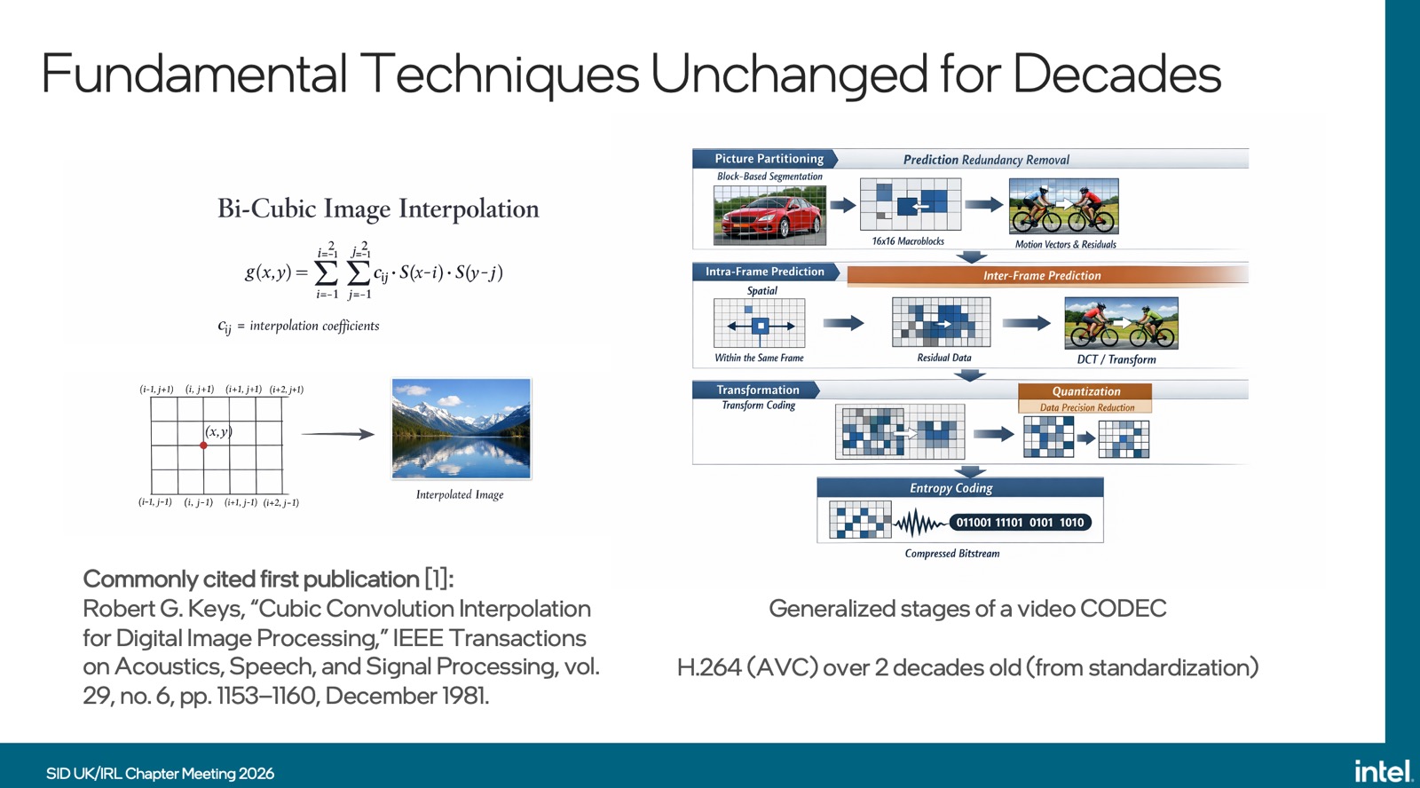
AI is being used already in video processing including, for example, upscaling of existing SD content to HD or even UltraHD. It was used in a demonstration of 8K streaming by Intel in association with the 8K Association during the last Olympics where AI was used to optimise the compression process. Cope highlighted during discussions that the 8K video was transmitted at an average of 20Mbps using the VVC codec developed by Spin Digital GmbH.
In practical applications, such as the use of video in tracking retail transactions, better AI-based scaling can help to improve object detection. Cope showed the results from a test comparing AI processed and non-processed identification at lower bit rates.
The full power in the new systems comes from a combination of CPUs, GPUs and NPUs to achieve high levels of performance. Which is best depends on the balance of need for low latency, power or power consumption.
EuroDisplay, AGM and Ben Sturgeon Intermission
Sam Phenix then gave details of the EuroDisplay conference which will take place from 22nd to 24th of September in Dublin, Ireland. Special rates for the conference hotel are currently available.
Tim Large conducted the formal business of the AGM for the UK chapter including the election of a new committee, which he will chair.
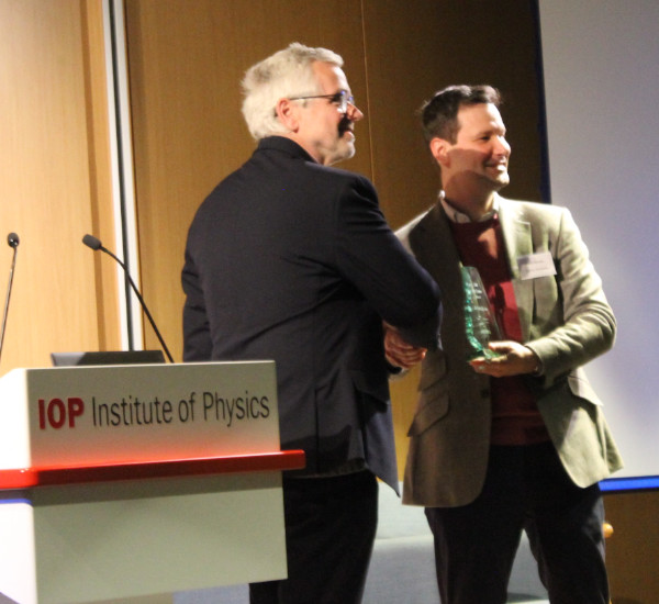
Prof Radu A. Sporea of Surrey University was awarded the Ben Sturgeon prize for his work on new transistor types used in displays and he explained the technology. The prize is awarded to young researchers in the display field which the UK chapter defines as work carried out before the age of 40.
New Transistors Offer Key Advantages vs LTPO
Sporea’s key work was on the source-gated transistor (SGT), the idea for which was first in a published paper in 2003 (IEEE Electron Device Letters, Vol 24. No 6, June 2003 ‘Source-gated Thin-Film Transistors’). The concept is to add a layer that controls the current in a Field Effect Transistor (FET) in the source rather than at the drain. The layer appears to reduce the efficiency of the transistor but allows you to do different things.
 He started by saying that his talk summarised around eight years of collaborative work, not least with Eva Bestelink of the UK chapter.
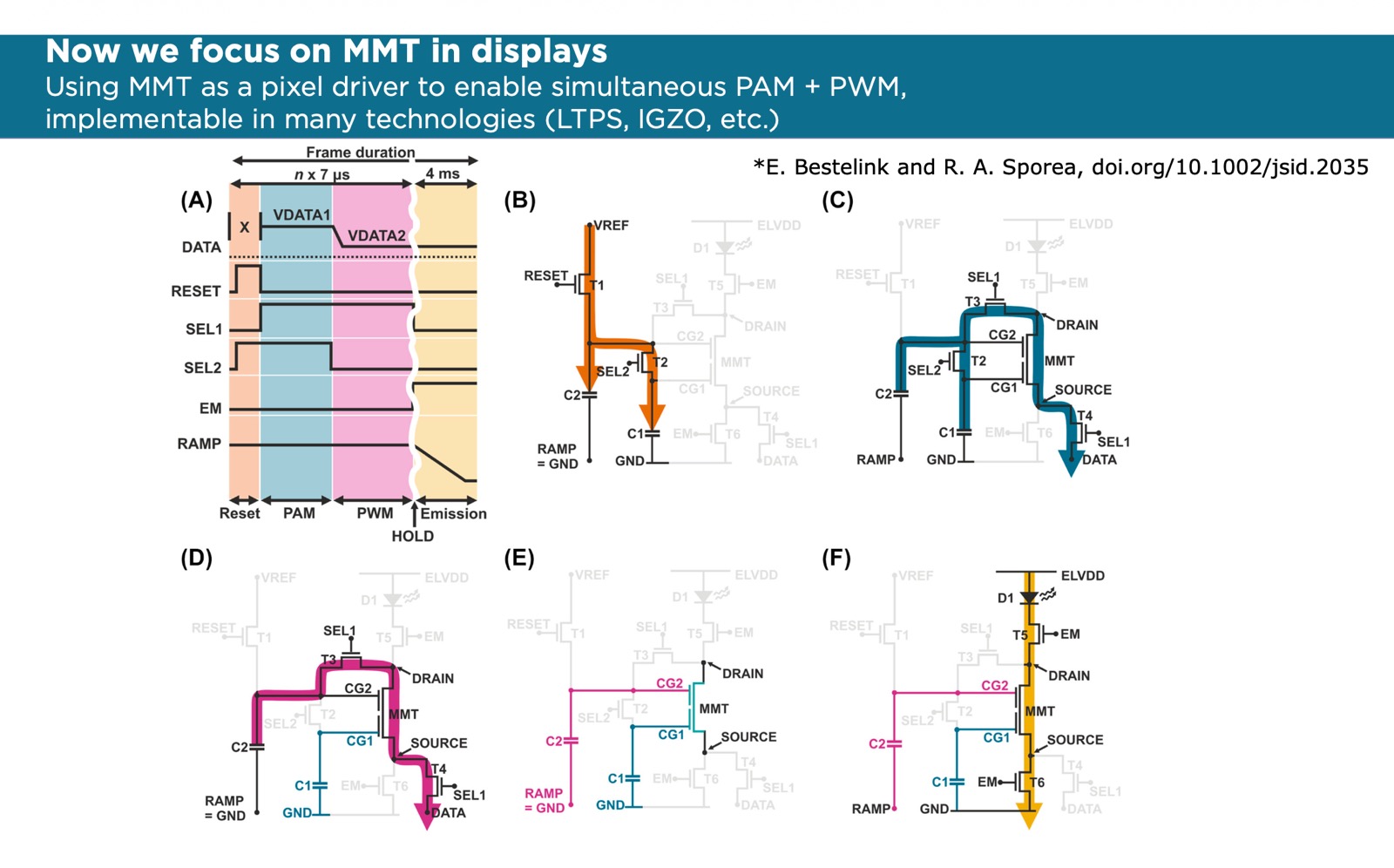
The Multimodal transistor (MMT) is a development of the SGT with two distinct control areas, one for current and one for the timing of current flow. One gate (CG1) exclusively controls the injection process while CG2 controls the conductivity of the channel. It’s a series process.
The devices can be made with all kinds of materials including polysilicon and IGZO and there are relatively simple design rules. Whatever is available in the technology can be exploited to support the CG2 barrier. You need a thin high K semiconductor and a relatively thick lower K dielectric. This allows the output curves to saturate at significantly lower voltage.
Using polysilicon, you can create something that is very close to an ideal current source. That source could be used to drive an emissive pixel, but can also be used in an amplifier configuration.
Sporea looked at the operation of simple two LTPS SGT-based devices which allow very high levels of gain. This can make the transistors very useful for sensor applications.
He then looked at work on organic source-gated phototransistors and he said that the characteristics are more consistent using a CCT (contact-controlled) transistor. He described a three transistor configuration that can be used to create a very sensitive temperature sensor. The temperature sensitivity by manipulating the dimensions of the transistor and the performance is available at different common voltages so careful power supply is not needed.
The work on pixel drivers is at a relatively early stage but there are already significant advantages. Again, there is relatively less dependence on power supply conditions.
The MMTs have significantly better performance in IT and possibly smartphone displays.
In smartphones, in particular, LTPO has been adopted to allow low refresh rates and improved power efficiency. As he explained, Oxides have very good off-current, but LTPS has very good on-current, which is why the combination is used. Source-gated transistors can offer an alternative.
In principle, LTPS only 1Hz devices are possible using contact controlled transistors. This could give significant production advantages over LTPO.
With this kind of contact controlled transistor there is a trade off of speed and current density for gain, stability and uniformity. Although there may appear to be shortcomings, these can be bypassed by elegant design solutions.
Multimodal transistor is a more refined version than the SGT with two control gates (CG). CG1 controls current flowing through the device, but CG2 controls the timing of that current.
Organic transistors can be used and have a very low off current. Sporea likened the CGs to a hose system, where the tap controls the level of water available, while a sprinkler control dictates when the water will flow. He described the different response curves of CG1 and CG2 and shows the independence of the two gates.
In display applications, Sporea’s group have developed a 7T2C (6T1M2C) pixel driver which can offer simultaneous pulse amplitude (PAM) and width (PWM) modulation and that can be an advantage in many displays using LTPS, IGZO or even amorphous silicon.
Quoting data from Hendy Consulting, Sporea highlighted the big saving in capex moving from LTPO to LTPS. This could be as much as $724 million for a G6 fab with 30K substrates/month throughput.
The technology also has applications in sensors and in AI applications.
Merck is Using Reactive Mesogens for Optical Films
 Nina Podoliak is from Southampton where she is working for Merck Performance Materials in the area of reactive mesogens (RMs) for optical films, especially for waveguides in augmented reality (AR) headsets.
AR development really started in 1968 or so, but the key moment was the arrival of Google Glass in 2014. Podoliak covered the differences between AR and VR. You need different optical elements for each of these and she went through the challenges, of which there are many.
For AR glasses, the image needs to be generated, coupled to the optics then output to the user’s eye. To get some scaling, you usually need more optics. Podoliak highlighted nine key challenges including cost.
She looked at the basic principles of operation from image generation, coupling to the waveguide and the outcoupling. The waveguide also be thin and transparent. Goals for the system include wide field of view (FOV), large eye box, high efficiency, good colour and low levels of stray light.
There are two kinds of main waveguides used. Geometric (based on embedded mirrors or prisms) optics are used by Meta. The other kind is the diffractive type and there are multiple different types. There are four main diffraction types
- Surface relief gratings
- Volume holographic gratings
- Metamaterial gratings
- Polarization volume holograms (PVH)
Podoliak went through the pros and cons of each approach.
The group is working on PVH solutions based on the use of reactive mesogens which are polymerizable LC materials. In these materials they can be aligned as liquids and after the LC phase can be turned into a durable plastic film which maintains the alignment. UV light is typically used. The materials can be anisotropic with controllable properties and are already used in compensation films, for example.
One of the uses for the films is the creation of Pancharatnam-Berry (PB) gratings which have high diffraction efficiency. RMs can be used to make multi-layer or multi-slant devices. Photo-alignment can be used to create different alignments of the LC materials and additional layers can be simply added without intermediate processing. Different manufacture methods include slot die coating and ink-jet printing so fabrication is straightforward.
There are two key control dimensions. You can control the pitch of the grating at the surface and you can also control the type of material used which can control the degree of chirality from chiral to non-chiral. These options allow a range of solutions based on dual axis grid.
Configurations can be made that split light into two circular polarised streams that will be emitted in different directions according to the PB pitch. The material type can control between the Raman-Nath and Bragg regimes. The technology can be used to make reflective or transmissive lenses and PVHs.
Podoliak turned to a comparison of SRGs vs PVH devices. While SEGs are sensitive to linear polarisation, PVH respond to circular. With SRGs, it is hard to eliminate unwanted effects. PVHs can match the light chirality to the material chirality and you can achieve polarisation multiplexing for each eye using the chirality.
You can reduce eye glow (the stray light going away from the eye in AR glasses) by introducing slant in the outcoupling grating. In PVH, the grating automatically reduces eye glow whereas using SRGs, it is difficult to eliminate.
PVHs can give higher in-coupling efficiency also reducing second interaction loss. Podoliak went through the different processes at in- and outcoupling.
Turning to broadband and uniformity, with SRGs there are usually trade-offs between efficiency and angular uniformity, so higher efficiency can be achieved, but at the cost of a smaller FOV.
PVH can be engineered for better angular range and efficiency because of the possibility of multilayer, multi-slant gratings. There is more flexibility to achieve waveguide optimisation.
Podoliak explained that PVH not yet an industrialised process. Material can be photoaligned which is a mass production process. RMs can be deposited with inkjets and can then be polymerised.
Sky Working to Improve TV Efficiency